Semiconductor Diode - Forward Bias And Reverse Bias

Semiconductor Diode - Forward Bias And Reverse Bias

Edited By Vishal kumar | Updated on Jul 02, 2025 06:09 PM IST

Consider the charger you use to power your smartphone. Inside that small device lies a crucial component known as a semiconductor diode. This diode ensures that electricity flows correctly, protecting your device from potential damage. A semiconductor diode can control the direction of current flow, which is essential for the functioning of electronic circuits.

This Story also Contains
  1. Semiconductor Diode
  2. P-N Junction Diode Under Forward Bias
  3. P-N Junction Diode Under Reverse Bias
  4. Formation of a Reverse Bias Diode
  5. Critical Value of Reverse Bias Voltage
  6. Experimental Study of the V-I characteristics of a Semiconductor Diode
  7. Solved Examples Based on Semiconductor Diode - Forward Bias And Reverse Bias
  8. Summary
Semiconductor Diode - Forward Bias And Reverse Bias

To understand how a semiconductor diode operates, we need to look at its two main modes: forward bias and reverse bias. These modes dictate how the diode allows or restricts the flow of electrical current, playing a vital role in rectification, signal modulation, and protection in electronic circuits. Let's explore how forward bias and reverse bias with the help of a solved example.

Semiconductor Diode

If a p-n junction has metallic contacts at both the ends for application of external voltage. This is called a semiconductor diode.

w3c4yPZ0dpJikVNIzs7Ilgaw9SImO9F_prVU_ZAOv60

The symbolical representation of a semiconductor diode is shown below -

1FlTmRishtte2xc5qUMjiX_ShwLCX7Z-TJFvLb6aEAg

In the figure given above, the arrow indicates the direction of current when the diode is under forward bias. One should note here that the equilibrium barrier potential can be altered. This can be done by applying an external voltage across the diode. Depending on how this voltage is applied, the diode is a forward-bias or a reverse-bias diode which we will study in the upcoming concept.

P-N Junction Diode Under Forward Bias

72IEORTJzUCEKLrQiHw5NdBkpbop2OmMIqz4Eg3WWbQ

In the figure given above, we can see that an external voltage is applied across the semiconductor diode where the p-side of the diode is connected to the positive terminal and the n-side is connected to the negative terminal of the battery. This type of arrangement for the diode is forward-biased.

Formation of a Forward Bias Diode

As the depletion region has no charge so the resistance is very high there so the applied voltage drops primarily across this region. The drop in voltage across the p and n side of the junction is relatively negligible. And the direction of the applied voltage (V) being opposite to that of the built-in potential (Vo) due to which the depletion layer’s width decreases and the barrier height reduces.

If the applied voltage is small, then the barrier potential is reduced marginally only below the equilibrium value. Then only small number of carriers crossing the junction, so the current is small. Similarly for a significantly high value of voltage, more carriers have the energy to cross the junction so, the current will be high.

One should also note that when the voltage is applied, some electrons cross to the p-side and some holes cross to the n-side. Under forward bias, this process is the minority charge injection process. Hence, the minority charge concentration which is electrons on the p-side are a minority and holes on the n-side are a minority, is significantly higher at the junction boundary.

Q8tPh5ilZUMikbWafC5ecsJO_r24P3k6kS-WIyHm9Kg

Due to this concentration gradient, the injected electron diffuse from the junction-end to the far-end of the p-side. Similarly, injected holes diffuse to the far end of the n-side. This gives rise to current too.

The total diode forward current = Hole diffusion current + Electron diffusion current (mA)

P-N Junction Diode Under Reverse Bias

_Eqy7NApkVeuqUb5nXNIB6CBzAWhNZkHQzARQFRQedk

In the figure given above, we can see that an external voltage is applied across the diode. We can see that the n-side of the diode connects to the positive terminal and the p-side connects to the negative terminal of the battery. This type of arrangement in the diode is a reverse-bias diode.

Formation of a Reverse Bias Diode

As the depletion region has no charges, the resistance will be very high, as a result, the applied voltage drops primarily across this region. Also, the drop in voltage across the p and n sides of the junction is relatively negligible. Now here the direction of the applied voltage (V) is the same as that of the built-in potential (V0) (Opposite to the forward bias), because of this the depletion layer’s width widens and the barrier height also increases. This decreases the flow of electrons to the p-side and holes to the n-side. So, the diffusion current decreases to a great extent.

Because of the direction of the electric field, the electrons in the p-side and holes in the n-side are driven to their majority zones, if they come close to the junction. This will produce the drift current. The drift current is usually of a few microamperes. This current is very low even in the forward-biased diode as compared to the current due to the injected carriers.

Critical Value of Reverse Bias Voltage

A small amount of voltage applied to the diode is sufficient to sweep the minority charge carrier to the far side of the junction. This diode reverses current which is not dependent on the voltage but on the concentration of the minority charge carriers on both sides of the junction. However, the current is independent up to a critical value of reverse bias voltage which is the Breakdown Voltage (Vbr). When the voltage applied crosses breakdown voltage i.e., Vbr, even a small change in the bias voltage causes a huge change in current. There is an upper limit of current for every diode, beyond which the diode gets destroyed due to overheating. This is the rated value of the current.

Experimental Study of the V-I characteristics of a Semiconductor Diode

pJorYFLl6BBcV4K_725iBxON4KZCqIdKCi3JDteecgE

OrSdPE8uwFQbJZeU4uq9-Zwqznqa396MgrIhRZVCN5I

V-I Characteristics of Diode

The figure shows a diode connected in reverse bias. The battery connects to the diode through a potentiometer by which we can change the voltage for the sake of the experiment. A microammeter is also used (since the expected current is in milliAmpere) to measure the current.

Here is the result of the experiment

kEPei6hz2fk6jStgS3LmbzAeJuk62G42ogKtfHlPXd8

As we can see in the graph above, in the forward biased diode, initially when the current increases almost negligibly till a certain value is reached. After that, the current increases exponentially even for a small increase in diode bias voltage. This voltage is called as threshold voltage. (Its value is approximately ~0.7 V for silicon diode and ~ 0.2 V for germanium diode)

In the reverse biased diode, the current is very small and almost remains constant with a change in bias voltage. It is called as Reverse saturation current. It is observed that in some cases, beyond the breakdown voltage, the current increases suddenly.

Hence, from this experiment and the given graph, we can conclude that the p-n junction diode allows the flow of current only in one direction, i.e. forward-bias, which means that the forward bias resistance is lower than the reverse bias resistance.

Extra edge -

1. P -N junction as diode

R = 0 , Forward
R → ∞ Reverse

It is a one-way device. It offers a low resistance when forward-biased and high resistance when reverse-biased.

2. Dynamic Resistance

Since slope of potential vs current graph is non uniform hence resistance keep changing .

R d = d v d i

download%20(1)

3. Knee voltage of P-N junction

Knee voltage for Ge is 0.3 V

Knee voltage for Si is 0.7 V

It is defined as the forward voltage at which the current through the junction starts rising rapidly with an increase in voltage.

4. Relation between current I & Voltage V

K = Boltzmann constant
I 0 = reverse saturation current
In forward bias

$

e^{\frac{\varepsilon v}{K T}}>>1

$

Then forward biasing current is

$

\begin{aligned}

& I=I_0 \cdot e^{\frac{\varepsilon v}{K T}} \\

& I=I_0\left(e^{\frac{c v}{K T}}-1\right)

\end{aligned}

$

Solved Examples Based on Semiconductor Diode - Forward Bias And Reverse Bias

Example 1: In an unbiased n-p junction electrons diffuse from n-region to p - region because :

1) holes in p - region attract them

2) electrons travel across the junction due to potential difference

3) electron concentration in n - region is higher as compared to that in p - region

4) only electrons move from n to p region and not the vice - versa

Solution:

In an unbiased p-n junction, electrons diffuse from the n-region to the p-region because of a concentration gradient.

Hence, the answer is the option (3)

Example 2: The circuit has two oppositely connected ideal diodes in parallel. What is the current (in ampere) following in the circuit?

5664_0_image

1) 2.00

2) 1.71

3) 1.33

4) 2.31

Solution:

P -N junction as diode

It is a one-way device. It offers a low resistance when forward-biased and high resistance when reverse-biased.

wherein

R = 0, Forward

R→∞ Reverse

Diode D1 is in reverse bias and hence this branch will offer infinite resistance and hence we can remove this.

Diode D2 is forward bias and hence it offers no resistance.

The circuit can be reduced to
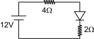
15

I=126=2A

The correct option is 1.

Example 3: If in a $p-n$ junction diode, a square input signal of 10 V is applied as shown

5665_1_image

Then the output signal will be

1)

20049_0_image

2)

20050_0_image

3)

20051_0_image

4)

20052_0_image

Solution:

P -N junction as diode

It is a one-way device. It offers a low resistance when forward-biased and high resistance when reverse-biased.

wherein

R=0, Forward
R→∞ Reverse
For - ve applied voltage the diode is in reverse biased mode and hence there is no current output across RL=0

If + 5V is applied, the diode is in forward-biased mode and hence offers no resistance.

Output voltage = 5V

Example 4: The forward-biased diode connection is :

1)

13793_0_image

2)

13794_0_image

3)

13795_0_image

4)

13796_0_image

Solution:

To determine which diode connection is forward-biased, we need to identify the configuration where the anode (positive side of the diode) is at a higher potential than the cathode (negative side of the diode).

Let's analyze each option:

  1. +2V on the anode and -2V on the cathode:

The voltage across the diode is +2V−(−2V)=+4V+2V - (-2V) = +4V+2V−(−2V)=+4V

This means the anode is at a higher potential than the cathode.

Forward-biased.

  1. -3V on the anode and -3V on the cathode:

NEET Highest Scoring Chapters & Topics
This ebook serves as a valuable study guide for NEET exams, specifically designed to assist students in light of recent changes and the removal of certain topics from the NEET exam.
Download E-book

The voltage across the diode is −3V−(−3V)=0V-3V - (-3V) = 0V−3V−(−3V)=0V.

The anode and cathode are at the same potential.

Not forward-biased.

  1. 2V on the anode and 4V on the cathode:

The voltage across the diode is 2V−4V=−2V2V - 4V = -2V2V−4V=−2V.

This means the anode is at a lower potential than the cathode.

Not forward-biased.

  1. -2V on the anode and +2V on the cathode:

The voltage across the diode is −2V−2V=−4V-2V - 2V = -4V−2V−2V=−4V.

This means the anode is at a lower potential than the cathode.

Not forward-biased.

Therefore, the forward-biased diode connection is:

Option 1).

Example 5: A 2V battery is connected across AB as shown in the figure. The value of the current supplied by the battery when in one case battery’s positive terminal is connected to A and in other case when the positive terminal of the battery is connected to B will respectively be :

3171_0_image

1) 0.2 A and 0.1 A

2) 0.4 A and 0.2 A

3) 0.1 A and 0.2 A

4) 0.2 A and 0.4 A

Solution:

3171

In one case
NO current will pass through D2
I=2/5 A=0.4 A

In the second case: no current will pass through D1
I=2/10=0.2 A

Summary

A junction of p-type and n-type semiconductors makes up a semiconductor. A p-side of the battery is positively linked to a p-type semiconductor while a pn junction connected to the n-side is negatively terminal. This means that the diode allows for the flow of electric current because the potential difference of the dopant atoms is decreased through frontward biasing. Nevertheless, by placing the p-side to the negative terminal and the n-side to the positive terminal refers to reverse biasing.

Frequently Asked Questions (FAQs)

1. What is the breakdown voltage of a diode?
The breakdown voltage is the reverse voltage at which a diode's ability to block current suddenly fails, allowing a large current to flow. This occurs due to either avalanche breakdown or Zener breakdown, depending on the diode's design and doping levels.
2. What is the difference between avalanche and Zener breakdown?
Avalanche breakdown occurs at higher voltages when accelerated electrons collide with atoms, creating more electron-hole pairs in a chain reaction. Zener breakdown happens at lower voltages due to quantum tunneling of electrons across the narrow depletion region in heavily doped diodes.
3. How does a varactor diode utilize the voltage-dependent capacitance?
A varactor diode is designed to exploit the voltage-dependent capacitance of a reverse-biased diode. By varying the reverse bias voltage, the capacitance can be controlled, making varactor diodes useful in tuning circuits and voltage-controlled oscillators.
4. What is the recovery time of a diode, and why is it important?
Recovery time is the time it takes for a diode to switch from conducting (forward bias) to non-conducting (reverse bias) state. It's important in high-frequency applications as it limits the maximum operating frequency of the diode.
5. What is the purpose of a freewheeling diode in a circuit?
A freewheeling diode, also called a flyback diode, is used in circuits with inductive loads to provide a path for current when the power is switched off. It prevents high voltage spikes that can damage other components in the circuit.
6. What is the knee voltage (or threshold voltage) of a diode?
The knee voltage, also called the threshold voltage, is the minimum forward voltage required for a diode to conduct significant current. It's typically around 0.7V for silicon diodes and 0.3V for germanium diodes. Below this voltage, the diode conducts very little current.
7. Why is there a small current in reverse bias called leakage current?
Leakage current in reverse bias is caused by thermally generated electron-hole pairs in the depletion region. These charge carriers are swept across the junction by the electric field, creating a small but measurable current even when the diode is supposed to block current flow.
8. How does temperature affect a diode's behavior?
Increasing temperature reduces the diode's forward voltage drop and increases its reverse leakage current. This is because higher temperatures increase the number of thermally generated charge carriers, making it easier for current to flow in both directions.
9. How does doping concentration affect a diode's characteristics?
Higher doping concentrations decrease the width of the depletion region, lower the forward voltage drop, and increase the reverse breakdown voltage. Lower doping concentrations have the opposite effects.
10. Why does current flow easily in forward bias but not in reverse bias?
In forward bias, the applied voltage pushes electrons from the n-type region and holes from the p-type region towards the junction, reducing the depletion region and allowing current flow. In reverse bias, the voltage pulls electrons and holes away from the junction, widening the depletion region and blocking current flow.
11. How does reverse bias work in a semiconductor diode?
Reverse bias occurs when a negative voltage is applied to the p-type region and a positive voltage to the n-type region. This increases the potential barrier at the p-n junction, preventing the flow of current through the diode, except for a small leakage current.
12. How does the width of the depletion region change with bias?
The depletion region width decreases in forward bias as the applied voltage pushes charge carriers towards the junction. In reverse bias, the width increases as the voltage pulls charge carriers away from the junction, expanding the region of immobile ions.
13. What is the purpose of a clamping diode in a circuit?
A clamping diode is used to limit the voltage in a circuit to a predetermined level. It conducts when the voltage exceeds this level, effectively "clamping" the voltage and protecting other components from overvoltage.
14. What is the difference between soft and hard breakdown in diodes?
Soft breakdown, typical in Zener diodes, is a controlled and non-destructive breakdown that occurs at a specific voltage. Hard breakdown, which can occur in any diode at high enough voltages, is potentially destructive and can permanently damage the device.
15. How does a Zener diode maintain a constant voltage in a circuit?
A Zener diode is operated in reverse breakdown mode, where it maintains a nearly constant voltage across it despite changes in current. This property makes it useful for voltage regulation and protection against voltage spikes.
16. What is forward bias in a semiconductor diode?
Forward bias is the condition when a positive voltage is applied to the p-type region (anode) and a negative voltage to the n-type region (cathode) of a diode. This reduces the potential barrier at the p-n junction, allowing current to flow easily through the diode.
17. What is the difference between majority and minority carrier injection in a forward-biased diode?
In a forward-biased diode, majority carriers (electrons in n-type, holes in p-type) are injected across the junction into regions where they become minority carriers. This minority carrier injection is crucial for current flow but also affects the diode's switching speed due to charge storage.
18. Why do LEDs have higher forward voltage drops than regular diodes?
LEDs (Light Emitting Diodes) have higher forward voltage drops because they're made from different semiconductor materials with larger band gaps. The larger band gap is necessary for emitting light but requires more energy (voltage) for electrons to cross.
19. What is the effect of series resistance on a diode's behavior?
Series resistance in a diode, often due to the semiconductor material and contacts, causes a voltage drop that adds to the junction voltage drop. This results in a more gradual increase in current with voltage in the forward bias region of the I-V curve.
20. How does a tunnel diode differ from a regular diode in terms of its I-V characteristics?
A tunnel diode exhibits negative differential resistance in part of its forward bias region, where current decreases as voltage increases. This is due to quantum tunneling effects and makes tunnel diodes useful in high-frequency oscillators and amplifiers.
21. What is the ideal diode model, and how does it differ from real diodes?
The ideal diode model assumes zero resistance and instant turn-on at 0V in forward bias, and infinite resistance in reverse bias. Real diodes have some forward resistance, require a threshold voltage to turn on, and have small leakage currents in reverse bias.
22. What is the capacitance of a diode, and how does it change with bias?
Diode capacitance is primarily due to the charge stored in the depletion region. It decreases with increasing reverse bias (as the depletion region widens) and increases with forward bias (as the depletion region narrows).
23. What is the difference between a pin diode and a regular p-n diode?
A pin diode has an intrinsic (undoped or lightly doped) layer between the p and n regions. This structure gives the diode variable resistance controlled by the forward bias current, making it useful in RF switching and attenuator applications.
24. How does avalanche noise in a reverse-biased diode differ from thermal noise?
Avalanche noise occurs in reverse-biased diodes near breakdown due to the random nature of charge carrier multiplication. It's typically larger and has a different frequency spectrum compared to thermal noise, which is present in all resistive components due to random thermal motion of charge carriers.
25. How does a diode's I-V characteristic curve illustrate its behavior?
The I-V characteristic curve shows the relationship between current (I) and voltage (V) in a diode. It typically shows an exponential increase in current for forward bias voltages above the knee voltage, and very little current (except for breakdown) in reverse bias.
26. What is a semiconductor diode?
A semiconductor diode is an electronic component made from a p-n junction, which allows current to flow easily in one direction (forward bias) but restricts flow in the opposite direction (reverse bias). It consists of two types of semiconductor materials: p-type and n-type, joined together to create a junction.
27. What is the depletion region in a semiconductor diode?
The depletion region is a narrow area at the p-n junction where free charge carriers (electrons and holes) have diffused across the junction and recombined, leaving behind immobile charged ions. This region acts as an insulator and creates a potential barrier that affects current flow.
28. How does the material of a diode (e.g., silicon vs. germanium) affect its properties?
Different materials have different band gaps and electron mobilities. Silicon diodes have a higher forward voltage drop (about 0.7V) but lower reverse leakage current compared to germanium diodes (about 0.3V forward drop). Silicon is more temperature-stable and can handle higher power.
29. How do Schottky diodes differ from regular p-n junction diodes?
Schottky diodes use a metal-semiconductor junction instead of a p-n junction. They have lower forward voltage drops (typically 0.2-0.3V), faster switching speeds, but higher reverse leakage currents compared to regular diodes.
30. How does the doping profile affect a diode's characteristics?
The doping profile (how doping concentration varies across the device) affects the electric field distribution in the diode. Uniform doping leads to a linear electric field, while non-uniform doping can create regions of high field strength, affecting breakdown voltage and capacitance.
31. How does reverse recovery time affect a diode's high-frequency performance?
Reverse recovery time is the time taken for a diode to stop conducting when switched from forward to reverse bias. Longer recovery times limit the diode's ability to switch quickly, reducing its effectiveness in high-frequency applications.
32. What is the purpose of a guard ring in a high-voltage diode?
A guard ring is a structural feature in high-voltage diodes designed to spread out the electric field at the edges of the junction. This prevents premature breakdown at the edges and increases the overall breakdown voltage of the device.
33. How does the choice of semiconductor material affect a diode's radiation hardness?
Different semiconductor materials have varying resistance to radiation damage. For example, silicon carbide (SiC) diodes are more radiation-resistant than silicon diodes due to their wider bandgap and stronger atomic bonds, making them suitable for space and nuclear applications.
34. How does the presence of traps and recombination centers affect a diode's performance?
Traps and recombination centers in the semiconductor material can capture and release charge carriers, affecting the diode's current-voltage characteristics, leakage current, and switching speed. They can also introduce additional noise and reduce the device's efficiency.
35. What is the significance of the ideality factor in a diode's equation?
The ideality factor, typically between 1 and 2, indicates how closely a diode follows the ideal diode equation. A factor of 1 suggests that diffusion current dominates, while a factor closer to 2 indicates that recombination in the depletion region plays a significant role in current flow.
36. How does the built-in potential of a diode relate to its doping levels?
The built-in potential of a diode is the potential difference that naturally exists across the p-n junction due to the diffusion of charge carriers. It increases with higher doping levels on either side of the junction, as this creates a larger concentration gradient for diffusion.
37. What is the effect of surface states on a diode's characteristics?
Surface states are energy levels at the semiconductor surface that can trap charge carriers. They can affect the diode's leakage current, breakdown voltage, and noise characteristics. Proper surface passivation techniques are used to minimize these effects.
38. How does carrier lifetime affect a diode's switching speed and reverse recovery time?
Carrier lifetime is the average time a minority carrier exists before recombining. Longer lifetimes result in more stored charge in forward bias, leading to slower switching speeds and longer reverse recovery times. Shorter lifetimes improve these parameters but may increase forward voltage drop.
39. What is the difference between drift and diffusion currents in a diode?
Drift current is caused by the electric field in the depletion region moving charge carriers. Diffusion current results from the concentration gradient of charge carriers across the junction. In forward bias, diffusion current dominates, while in reverse bias, drift current (of minority carriers) is more significant.
40. How does the presence of deep-level impurities affect a diode's reverse leakage current?
Deep-level impurities introduce energy states near the middle of the semiconductor's bandgap. These states can act as generation-recombination centers, facilitating the thermal generation of electron-hole pairs in the depletion region, which increases the reverse leakage current.
41. What is the impact of series inductance on a diode's high-frequency behavior?
Series inductance, often from the diode's leads and packaging, can limit the device's high-frequency performance. It creates a reactive impedance that increases with frequency, potentially causing ringing or oscillations in fast-switching applications.
42. How does the choice of contact metal affect a diode's characteristics?
The choice of contact metal affects the diode's series resistance and can create a Schottky barrier at the metal-semiconductor interface. Proper selection ensures low-resistance ohmic contacts for regular diodes, while specific metals are chosen to create desired Schottky barrier heights in Schottky diodes.
43. What is the difference between abrupt and graded junctions in diodes?
Abrupt junctions have a sharp transition between p and n regions, while graded junctions have a gradual change in doping concentration. Graded junctions typically have lower capacitance and higher breakdown voltages but may have higher series resistance compared to abrupt junctions.
44. How does self-heating affect a diode's characteristics during operation?
Self-heating occurs due to power dissipation in the diode. It can increase the diode's temperature, leading to lower forward voltage drop, higher reverse leakage current, and potentially altered breakdown characteristics. Excessive self-heating can lead to thermal runaway and device failure.
45. What is the significance of the depletion capacitance in reverse-biased diodes?
Depletion capacitance in reverse-biased diodes arises from the charge stored in the depletion region. It's voltage-dependent and decreases with increasing reverse bias. This capacitance is crucial in applications like varactor diodes and affects the diode's high-frequency behavior.
46. How does carrier velocity saturation affect a diode's behavior at high electric fields?
At high electric fields, charge carriers reach a maximum velocity due to increased scattering. This velocity saturation limits the current increase with voltage, causing the diode's I-V characteristic to deviate from the ideal exponential relationship at high current levels.
47. What is the impact of surface recombination on a diode's performance?
Surface recombination occurs when charge carriers recombine at the semiconductor surface due to surface defects or dangling bonds. It can increase leakage current, reduce quantum efficiency in optoelectronic devices, and affect the diode's overall current-voltage characteristics.
48. How does bandgap narrowing in heavily doped regions affect a diode's behavior?
Bandgap narrowing occurs in heavily doped semiconductor regions, reducing the effective bandgap. This can lead to increased intrinsic carrier concentration, affecting the diode's reverse leakage current and forward voltage characteristics, particularly in devices with very high doping levels.
49. What is the effect of interface states in heterojunction diodes?
Interface states in heterojunction diodes (made from two different semiconductor materials) can trap charge carriers at the junction interface. This can lead to non-ideal current-voltage characteristics, increased leakage current, and altered capacitance behavior compared to homojunction diodes.
50. How does carrier freeze-out affect diode behavior at very low temperatures?
Carrier freeze-out occurs at very low temperatures when there's insufficient thermal energy to ionize dopant atoms. This reduces the number of free carriers, increasing the diode's resistance and altering its I-V characteristics. The effect is more pronounced in semiconductors with deeper dopant energy levels.

Articles

Back to top