Types Of Semiconductor: Intrinsic And Extrinsic Semiconductor

Types Of Semiconductor: Intrinsic And Extrinsic Semiconductor

Edited By Vishal kumar | Updated on Jul 02, 2025 05:45 PM IST

Imagine the electronic devices you use every day—your smartphone, laptop, or even the LED lights in your home. All these devices rely on a special class of materials called semiconductors to function. Semiconductors are essential because they have properties that fall between those of conductors (like copper) and insulators (like glass). This unique property allows them to control electrical currents, making them the backbone of modern electronics.

This Story also Contains
  1. What is Intrinsic Semiconductor?
  2. What is Extrinsic Semiconductor?
  3. Solved Examples Based on Types Of Semiconductor: Intrinsic And Extrinsic Semiconductor
  4. Summary
Types Of Semiconductor: Intrinsic And Extrinsic Semiconductor

Now, let's dive into the two main types of semiconductors: intrinsic and extrinsic semiconductors. Understanding these types will give you insight into how semiconductors are engineered to meet the diverse needs of our electronic world.

What is Intrinsic Semiconductor?

It is a pure semiconductor. Silicon and germanium are the most common examples of intrinsic semiconductors. Both these semiconductors are most frequently used in the manufacturing of transistors, diodes and other electronic components.

Both Si and Ge have four valence electrons. In its crystalline structure, every Si or Ge atom tends to share one of its four valence electrons with each of its four nearest neighbour atoms, and also to take a share of one electron from each such neighbour as shown in the below figure. This shared pair of the electrons is called a Covalent bond or a Valence bond.

1674191242896

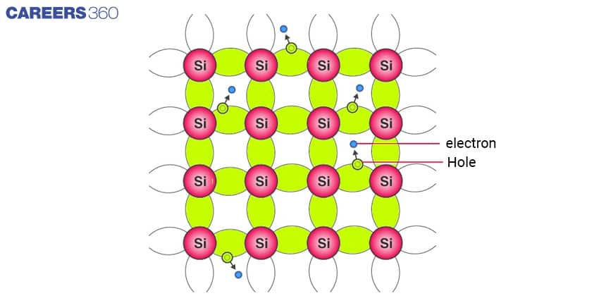
The above figure shows the structure with all bonds intact (i.e. no bonds are broken). This is possible only at low temperatures. As the temperature increases, more thermal energy becomes available to these electrons and some of these electrons may break–away from the conduction band becoming the free electron and creating a vacancy in the bond. This vacancy with an effective positive electronic charge is called a hole.

In intrinsic semiconductors, the number of free electrons ( ne ) is equal to the number of holes ( nh )

i.e ne=nh=ni where ni is called intrinsic carrier concentration.

Semiconductors possess the unique property in which, apart from electrons, the holes also move. The free-electron moves completely independently as a conduction electron and gives rise to an electron current, Ie under an applied electric field. while Under an electric field, these holes move towards the negative potential generating hole current (Ih).

Hence, the total current (I) is given as I=Ie+Ih

Apart from the process of generation of conduction electrons and holes, a simultaneous process of recombination occurs in which the electrons recombine with the holes. At equilibrium, the rate of generation is equal to the rate of recombination of charge carriers.

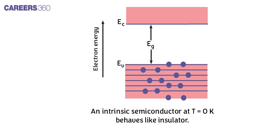
An intrinsic semiconductor will behave like an insulator at T = 0 K. As shown in the below figure., at T = 0 K, the electrons stay in the valence band and there is no movement to the conduction band.

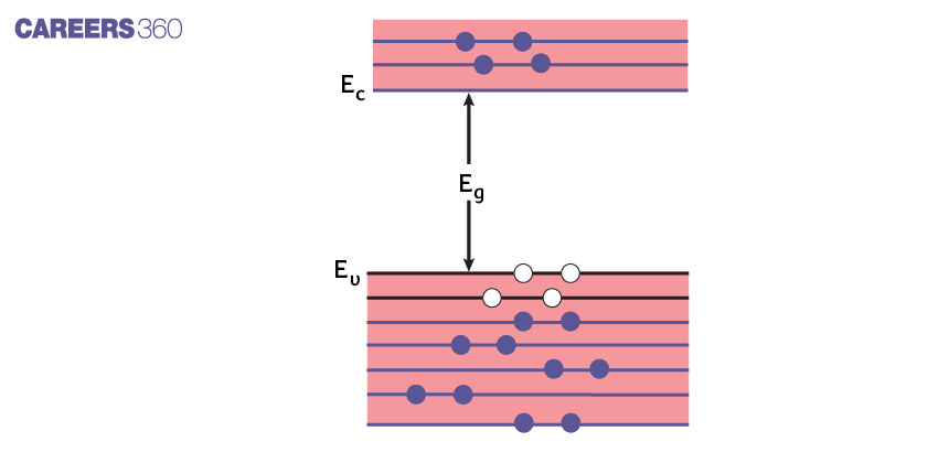
When the temperature increases, at T > 0K, some electrons get excited. These electrons jump from the valence to the conduction band as shown in the below figure.


The conductivity of an intrinsic semiconductor at room temperature is very low. As such, no important electronic devices can be developed using these semiconductors. Hence there is a necessity of improving their conductivity. This can be done by making use of impurities. because when a small amount of a suitable impurity is added to the pure semiconductor, the conductivity of the semiconductor is increased manifold

What is Extrinsic Semiconductor?

An extrinsic semiconductor is a semiconductor doped by a specific impurity which is able to deeply modify its electrical properties, making it suitable for electronic applications. The deliberate addition of a desirable impurity is called doping and the impurity atoms are called dopants. Another term for Extrinsic semiconductors is ‘Doped Semiconductor’.

The size of the dopant and Semiconductor atoms should be the same, to make sure that the amount of impurity added should not change the lattice structure of the semiconductor.

The following types of dopants are used in doping the tetravalent (valency 4) Si or Ge:

(i) Pentavalent (valency 5); like Arsenic (As), Antimony (Sb), Phosphorous (P), etc. This will give an n-type semiconductor

(ii) Trivalent (valency 3); like Indium (In), Boron (B), Aluminium (Al), etc. This will give a p-type semiconductor

What is an n-type Semiconductor?

When a pentavalent impurity is added to an intrinsic or pure semiconductor (silicon or germanium), then it is said to be an n-type semiconductor. Pentavalent impurities such as phosphorus, arsenic, antimony, etc are called donor impurities.

The four valence electrons of each phosphorus atom form 4 covalent bonds with the 4 neighbouring silicon atoms. The free-electron (fifth valence electron) of the phosphorus atom does not involved in the formation of covalent bonds. This shows that each phosphorus atom donates one free electron. Therefore, all the pentavalent impurities are called donors.

So, there is a donor energy level between the valence band and the conduction band. Just below the conduction band.

The number of free electrons depends on the amount of impurity (phosphorus) added to the silicon.

Charge on n-type Semiconductor

Even though an n-type semiconductor has a large number of free electrons, the total electric charge of an n-type semiconductor is neutral.

Conduction in n-type Semiconductor

When voltage is applied to n-type semiconductors as shown in the below figure; then the free electrons move towards the positive terminal of the applied voltage. Similarly, holes move towards the negative terminal of the applied voltage.

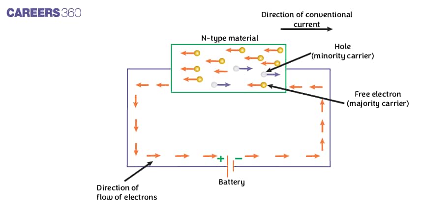
In an n-type semiconductor, conduction is mainly because of the motion of free electrons.

because In an n-type semiconductor, the population of free electrons is more whereas the population of holes is less (i.e. ne >>nh). In an n-type semiconductor, free electrons are called majority carriers and holes are called minority carriers.

What is a p-type semiconductor?

When the trivalent impurity is added to an intrinsic semiconductor (Si and Ge), then it is said to be a p-type semiconductor. Trivalent impurities such as Boron (B), Gallium (G), Indium(In), Aluminium(Al), etc are called acceptor impurities.

The three valence electrons of each boron atom form 3 covalent bonds with the 3 neighbouring silicon atoms.

For the fourth covalent bond, only the silicon atom contributes one valence electron. Thus, the fourth covalent bond is incomplete with the shortage of one electron. and This missing electron is called a hole.

This shows each boron atom accepts one electron to fill the hole. Therefore, all the trivalent impurities are called acceptors. So there is an acceptor energy level just above the valence band. A small addition of impurity (boron) provides millions of holes.

Charge on the P-Type Semiconductor

Even though p-type semiconductor has a large number of holes, the total electric charge of p-type semiconductors is neutral.

Conduction in p-type semiconductor

When voltage is applied to p-type semiconductor as shown in the below figure; then the free electrons move towards the positive terminal of the applied voltage. Similarly, holes move towards the negative terminal of the applied voltage.

In a p-type semiconductor, conduction is mainly because of the motion of holes in the valence band.

because In a p-type semiconductor, the population of free electrons is less whereas the population of holes is more (i.e nh >>ne)

In a p-type semiconductor, holes are called majority carriers and free electrons are called minority carriers.

Number of electrons or holes

The electron and hole concentration in a semiconductor in thermal equilibrium are related as:

ne × nh = ni2

On the increasing temperature, the number of current carriers increases.

The relation is given as ne=nh=AT32e−Eg2KT

where

Eg = Energy gap

K = Boltzmann Constant

T = Temperature in kelvin

Solved Examples Based on Types Of Semiconductor: Intrinsic And Extrinsic Semiconductor

Example 1: The conduction of electricity in intrinsic semiconductors is caused by.

1) The flow of electrons in the Conduction band only

2) The flow of holes in the Valence band only

3) Flow of electrons in the conduction band and flow of holes in the valence band.

4) None of these

Solution:

Intrinsic semiconductor

It is a pure semiconductor

e.g. pure Ge, or Pure Si

wherein

low conductivity

ne = nh

At room temperature, a few covalent bonds are broken due to thermal agitation. Thus, some of the valence electrons become free and shift to the valence band, leaving a space in the valence band of the intrinsic semiconductor's crystals. This electron-deficient space is known as a hole and it acts like a positively charged particle.

When an external electric field is applied across the semiconductor, the electrons present in the conduction band move opposite the direction of the electric field while the positive holes in the valence bond move in the direction of the external electric field. The movement of the electrons and holes causes the conduction of electricity in intrinsic semiconductors.

Hence, the answer is the option 3.

Example 2: The probability of electrons to be found in the conduction band of an intrinsic semiconductor at a finite temperature

1) increases exponentially with an increasing band gap

2) decreases exponentially with an increasing band gap

3) decreases with increasing temperature

4) is independent of the temperature and the band gap

Solution:

For an intrinsic semiconductor, at a finite temperature, the probability of electrons existing in the conduction band decreases exponentially with an increasing bandgap (Eg)
The relation is n=n0e−Eq/2k9T

where the Energy band gap
kB= Boltzmann's constant.

Hence, the answer is the option (2).

Example 3: In a semiconductor, the number density of intrinsic charge carriers 27∘C is 1.5×10¹⁶/m3. If the semiconductor is doped with an impurity atom, the hole density increases 4.5×10²²/m3. The electron density in the doped semiconductor is ×109/m3

1) 5

2) 4

3) 6

4) 3

Solution:

ni=1⋅5×1016/m3nh=4⋅5×1022/m3ne=?

We know that, Intrinsic change carrier density =ni=nhne
ni=nhne1⋅5×1016=4⋅5×1022×ne2⋅25×1032=4⋅5×1022×nene=0.5×10¹⁰ne=5×10⁹ m−3

Hence, the answer is option (1).

Example 4: What is the conductivity (in (Ω−m)−1 ) of a semiconductor sample having electron concentration of 5×10¹⁸ m−3, hole concentration of 5×10¹⁹ m−3, electron mobility of 2.0 m2 V−1 s−1 and hole mobility of 0.01 m2 V−1 s−1 ? (write your answer up to two decimals) (Take charge of electron as 1.6×10⁻¹⁹C )

1) 1.68

2) 1.83

3) 0.59

4) 1.20

Solution:

Electrical Conductivity ( σ )
σ=e(neμc+nhμh)
wherein
ne= electron density nh= hole density μe= mobility of electron μh= mobility of holes
Conductivity σ=e(neμe+nhμh)=1.6×10⁻¹⁹(5×1018×2+5×1019×0.01)=1.6×10⁻¹⁹(1019+0.05×10¹⁹)=1.6×1.05=1.68(Ω−m)−1

Hence, the answer is option (1).

Example 5: The ratio of electron and hole currents in a semiconductor is 7/4 and the ratio of drift velocities of electrons and holes is 5/4, then the ratio of concentrations of electrons and holes will be

1) 57
2) 75
3) 2549
4) 4925

Solution:

I=nAevd∴IcIh=ncvcnhvh or nenh=IcIh×vhve=74×45=75

Hence, the answer is the option (2).

Summary

Semiconductors, essential for modern electronics, are materials with properties between conductors and insulators. Intrinsic semiconductors are pure and have equal numbers of free electrons and holes, while extrinsic semiconductors are doped with impurities to enhance their conductivity, creating n-type (more free electrons) or p-type (more holes) semiconductors. Understanding these types explains the foundational principles behind electronic components like transistors and diodes.

Frequently Asked Questions (FAQs)

1. What is an extrinsic semiconductor?
An extrinsic semiconductor is a semiconductor material that has been doped with impurities to modify its electrical properties. The addition of impurities creates an imbalance in the number of electrons and holes, enhancing conductivity.
2. What are the two types of extrinsic semiconductors?
The two types of extrinsic semiconductors are n-type and p-type. N-type semiconductors have an excess of electrons as majority carriers, while p-type semiconductors have an excess of holes as majority carriers.
3. What is a semiconductor?
A semiconductor is a material with electrical conductivity between that of a conductor and an insulator. Its conductivity can be controlled by introducing impurities or applying external fields, making it crucial for electronic devices.
4. How is an n-type semiconductor created?
An n-type semiconductor is created by doping an intrinsic semiconductor with pentavalent impurities (donors) such as phosphorus, arsenic, or antimony. These impurities provide extra electrons, making electrons the majority carriers.
5. How does the band structure of a semiconductor differ from that of insulators and conductors?
Semiconductors have a small energy gap (band gap) between the valence band and conduction band, typically less than 3 eV. This is smaller than insulators (large gap) but larger than conductors (overlapping bands), allowing for controlled electrical properties.
6. What is an intrinsic semiconductor?
An intrinsic semiconductor is a pure semiconductor material without any impurities added. Its electrical properties are determined by the inherent crystal structure of the material, such as silicon or germanium.
7. How do electrons and holes contribute to conduction in intrinsic semiconductors?
In intrinsic semiconductors, thermal energy excites electrons from the valence band to the conduction band, creating an equal number of electrons and holes. Both charge carriers contribute to electrical conduction, moving in opposite directions under an applied electric field.
8. What is the Fermi level in an intrinsic semiconductor?
The Fermi level in an intrinsic semiconductor is located approximately in the middle of the band gap. It represents the energy level with a 50% probability of being occupied by an electron at thermal equilibrium.
9. How does temperature affect the conductivity of an intrinsic semiconductor?
As temperature increases, more electrons gain enough energy to jump to the conduction band, creating more electron-hole pairs. This increases the number of charge carriers, leading to higher conductivity in intrinsic semiconductors at higher temperatures.
10. Why is silicon more commonly used than germanium in semiconductor devices?
Silicon is more commonly used because it has a larger band gap (1.1 eV) compared to germanium (0.67 eV), making it more stable at higher temperatures. Silicon also forms a stable oxide layer, which is crucial for fabricating integrated circuits.
11. What is the Hall effect and how is it used to characterize semiconductors?
The Hall effect is the production of a voltage difference across a conductor when a magnetic field is applied perpendicular to the current flow. In semiconductors, it's used to determine the type of majority carriers (electrons or holes), their concentration, and mobility.
12. How does band bending occur at semiconductor surfaces and interfaces?
Band bending refers to the curvature of energy bands near semiconductor surfaces or interfaces. It occurs due to charge transfer or the presence of surface states, affecting the local electric field and carrier concentrations. This phenomenon is crucial in understanding device behavior at junctions and contacts.
13. What is the concept of quasi-Fermi levels in non-equilibrium conditions?
Quasi-Fermi levels describe the separate chemical potentials for electrons and holes when a semiconductor is not in thermal equilibrium, such as under illumination or current injection. They provide a way to describe carrier concentrations in these non-equilibrium conditions.
14. How do surface states affect the electrical properties of semiconductors?
Surface states are energy levels at a semiconductor's surface due to incomplete atomic bonding. They can trap charge, creating a surface charge and band bending. This affects carrier concentrations near the surface and can influence device behavior, especially in small-scale devices with high surface-to-volume ratios.
15. How do quantum wells modify the electronic properties of semiconductors?
Quantum wells are thin layers of a lower band gap semiconductor sandwiched between higher band gap materials. They confine carriers in one dimension, leading to quantized energy levels, modified density of states, and enhanced optical and electronic properties, which are exploited in lasers and high-electron-mobility transistors.
16. What is the concept of hot carriers in semiconductors and how do they affect device performance?
Hot carriers are charge carriers with energy significantly above the band edge. They can be created by high electric fields or optical excitation. Hot carriers can cause undesirable effects like impact ionization, carrier injection into gate oxides, and reduced device reliability. However, they're also exploited in some devices, such as hot-carrier solar cells.
17. How does bandgap engineering in semiconductor heterostructures enable novel device functionalities?
Bandgap engineering involves creating structures with varying compositions and band gaps. This allows for the control of carrier confinement, energy barriers, and band alignments. It enables the design of quantum wells, superlattices, and heterojunction devices with tailored electronic and optical properties, crucial for applications in lasers, high-electron-mobility transistors, and multi-junction solar cells.
18. What are donor atoms in n-type semiconductors?
Donor atoms are impurities added to create n-type semiconductors. They have one more valence electron than the atoms of the host semiconductor. This extra electron is easily ionized, becoming a free electron in the conduction band.
19. How is a p-type semiconductor created?
A p-type semiconductor is created by doping an intrinsic semiconductor with trivalent impurities (acceptors) such as boron, aluminum, or gallium. These impurities create holes in the valence band, making holes the majority carriers.
20. What are acceptor atoms in p-type semiconductors?
Acceptor atoms are impurities added to create p-type semiconductors. They have one fewer valence electron than the atoms of the host semiconductor. This creates a hole in the valence band, which can accept an electron from neighboring atoms.
21. How does doping affect the Fermi level in extrinsic semiconductors?
In n-type semiconductors, doping shifts the Fermi level closer to the conduction band. In p-type semiconductors, doping shifts the Fermi level closer to the valence band. This shift reflects the change in electron and hole concentrations.
22. What is the difference between majority and minority carriers in extrinsic semiconductors?
Majority carriers are the more abundant charge carriers resulting from doping. In n-type semiconductors, electrons are majority carriers; in p-type, holes are majority carriers. Minority carriers are the less abundant type, created through thermal excitation or light absorption.
23. How does the conductivity of extrinsic semiconductors compare to intrinsic semiconductors?
Extrinsic semiconductors have higher conductivity than intrinsic semiconductors at room temperature. This is because doping introduces a large number of charge carriers, significantly increasing the material's ability to conduct electricity.
24. What is charge neutrality in semiconductors?
Charge neutrality in semiconductors means that the total positive charge equals the total negative charge in the material. In intrinsic semiconductors, the number of electrons equals the number of holes. In extrinsic semiconductors, the sum of holes and ionized donors equals the sum of electrons and ionized acceptors.
25. How does light affect semiconductor conductivity?
Light can excite electrons from the valence band to the conduction band in semiconductors, creating electron-hole pairs. This process, called photoconductivity, increases the number of charge carriers and thus the conductivity of the semiconductor.
26. What is the depletion region in a p-n junction?
The depletion region is the area at the junction between p-type and n-type semiconductors where mobile charge carriers have diffused away. It contains fixed charged ions and acts as an insulator, creating a built-in electric field across the junction.
27. How does temperature affect extrinsic semiconductors differently from intrinsic ones?
At low temperatures, extrinsic semiconductors maintain higher conductivity due to the presence of dopants. As temperature increases, intrinsic carrier generation becomes more significant, and the behavior of extrinsic semiconductors approaches that of intrinsic ones at very high temperatures.
28. What is carrier recombination in semiconductors?
Carrier recombination is the process where electrons in the conduction band lose energy and return to the valence band, eliminating a hole. This can occur through various mechanisms, including radiative recombination (emitting a photon) or non-radiative recombination (releasing energy as heat).
29. How does doping concentration affect the width of the band gap?
Heavy doping can cause the band gap to narrow slightly. This effect, known as band gap narrowing, occurs due to the interaction between dopant atoms and the semiconductor's crystal structure, affecting the energy levels of the conduction and valence bands.
30. What is the difference between direct and indirect band gap semiconductors?
In direct band gap semiconductors, the minimum of the conduction band aligns with the maximum of the valence band in momentum space, allowing direct electron transitions. In indirect band gap semiconductors, these points are misaligned, requiring phonon assistance for transitions, which affects optical properties.
31. How does doping affect the position of the Fermi level in extrinsic semiconductors?
Doping shifts the Fermi level in extrinsic semiconductors. In n-type semiconductors, the Fermi level moves closer to the conduction band. In p-type semiconductors, it moves closer to the valence band. The exact position depends on the doping concentration and temperature.
32. What is compensation in semiconductors?
Compensation in semiconductors occurs when both donor and acceptor impurities are present in the same material. The donors and acceptors can partially cancel each other's effects, resulting in a reduced net doping level and altered electrical properties.
33. How does the concept of effective mass apply to charge carriers in semiconductors?
Effective mass is a concept used to describe how electrons and holes move within a semiconductor's crystal structure. It accounts for the interaction between charge carriers and the periodic potential of the crystal lattice, affecting carrier mobility and other transport properties.
34. What is the difference between shallow and deep level impurities in semiconductors?
Shallow level impurities introduce energy levels close to the band edges (conduction band for donors, valence band for acceptors) and are easily ionized at room temperature. Deep level impurities create energy levels deeper in the band gap, requiring more energy for ionization and often acting as recombination centers.
35. How does quantum confinement affect semiconductor properties in nanostructures?
Quantum confinement occurs when the size of a semiconductor structure approaches the de Broglie wavelength of charge carriers. This leads to discrete energy levels, widening of the band gap, and altered optical and electrical properties, which are exploited in quantum dots and other nanostructures.
36. How do impurity bands form in heavily doped semiconductors?
In heavily doped semiconductors, the wave functions of impurity atoms begin to overlap, forming an impurity band. As doping increases, this band can merge with the conduction or valence band, leading to degenerate semiconductor behavior similar to that of a metal.
37. What is the difference between drift and diffusion currents in semiconductors?
Drift current results from charge carriers moving under the influence of an electric field. Diffusion current arises from the movement of carriers from regions of high concentration to low concentration. Both contribute to the total current in semiconductor devices.
38. How does carrier freeze-out affect semiconductor behavior at low temperatures?
Carrier freeze-out occurs at low temperatures when there isn't enough thermal energy to ionize dopant atoms. This leads to a decrease in free carrier concentration and an increase in resistivity, affecting the semiconductor's electrical properties.
39. What is the difference between direct and indirect recombination processes in semiconductors?
Direct recombination involves an electron transitioning directly from the conduction band to the valence band, emitting a photon. Indirect recombination requires the assistance of a phonon to conserve momentum, making it a slower process. The type of recombination depends on the semiconductor's band structure.
40. How do trap states affect carrier lifetime and recombination in semiconductors?
Trap states are energy levels within the band gap caused by defects or impurities. They can capture and release carriers, affecting carrier lifetime and recombination rates. Deep-level traps often act as recombination centers, reducing carrier lifetime and device efficiency.
41. What is the concept of mobility in semiconductors and how is it affected by different scattering mechanisms?
Mobility describes how easily charge carriers move through a semiconductor under an applied electric field. It's affected by various scattering mechanisms, including lattice vibrations (phonon scattering), ionized impurity scattering, and carrier-carrier scattering. These mechanisms depend on temperature, doping concentration, and electric field strength.
42. How does heavy doping affect the optical properties of semiconductors?
Heavy doping can lead to band gap narrowing and increased free carrier absorption. It can also cause a shift in the absorption edge (Burstein-Moss shift) due to band filling. These effects alter the semiconductor's optical properties, including its refractive index and absorption spectrum.
43. What is the difference between equilibrium and non-equilibrium carrier concentrations in semiconductors?
Equilibrium carrier concentrations exist when a semiconductor is in thermal equilibrium, with carrier generation and recombination rates balanced. Non-equilibrium concentrations occur when external factors (like light or electrical injection) create excess carriers, leading to different electron and hole concentrations.
44. What is the concept of generation-recombination noise in semiconductors?
Generation-recombination noise arises from random fluctuations in carrier generation and recombination processes. It's particularly important in devices operating with small numbers of carriers and can limit the sensitivity of semiconductor detectors and the performance of low-noise amplifiers.
45. How does carrier lifetime vary between direct and indirect band gap semiconductors?
Carrier lifetime is generally longer in indirect band gap semiconductors compared to direct band gap semiconductors. This is because recombination in indirect band gap materials requires phonon assistance, making the process less probable and slower, leading to longer carrier lifetimes.
46. What is the impact of strain on semiconductor band structure?
Strain in semiconductors can modify the band structure, altering the band gap and carrier effective masses. Compressive strain typically reduces the band gap, while tensile strain increases it. This effect is used in band gap engineering for various applications, including improving the performance of transistors and optoelectronic devices.
47. What is the difference between majority and minority carrier injection in semiconductor devices?
Majority carrier injection involves the flow of majority carriers (electrons in n-type, holes in p-type) into a region where they remain majority carriers. Minority carrier injection involves the flow of minority carriers into a region where they are minority carriers. The latter is crucial for bipolar devices and solar cells, affecting recombination and device characteristics.
48. How does carrier concentration affect the position of the Fermi level in degenerate semiconductors?
In degenerate semiconductors, which have very high doping levels, the Fermi level moves into the conduction band (for n-type) or valence band (for p-type). This leads to metal-like behavior, with the semiconductor becoming more conductive and the Fermi level position depending strongly on the carrier concentration.
49. What is the role of phonons in carrier transport and recombination in semiconductors?
Phonons, which are quantized lattice vibrations, play crucial roles in semiconductors. They scatter carriers, affecting mobility and heat transport. In indirect band gap semiconductors, phonons assist in optical transitions and recombination processes by providing the necessary momentum for these events.
50. How do high electric fields affect carrier transport in semiconductors?
High electric fields can lead to velocity saturation, where carrier velocity no longer increases linearly with field strength. This occurs when carriers gain energy faster than they can lose it to the lattice. At even higher fields, impact ionization can occur, creating additional electron-hole pairs and potentially leading to avalanche breakdown.

Articles

Back to top